|
RomRaider
Documentation
Community
Developers
|
| Author |
Message |
|
eamiller
|
Post subject:  Posted: Posted: Thu Nov 16, 2006 12:01 am |
|
 |
| Newbie |
Joined: Sat Oct 07, 2006 9:46 pm
Posts: 10
|
|
Top Left
You do not have the required permissions to view the files attached to this post.
|
|
| Top |
|
 |
|
05GarnetLGT
|
Post subject: Posted: Thu Nov 16, 2006 12:15 am |
|
|
| Experienced |
Joined: Fri Feb 10, 2006 4:41 pm
Posts: 483
Location: toggle switch envy, PA
|
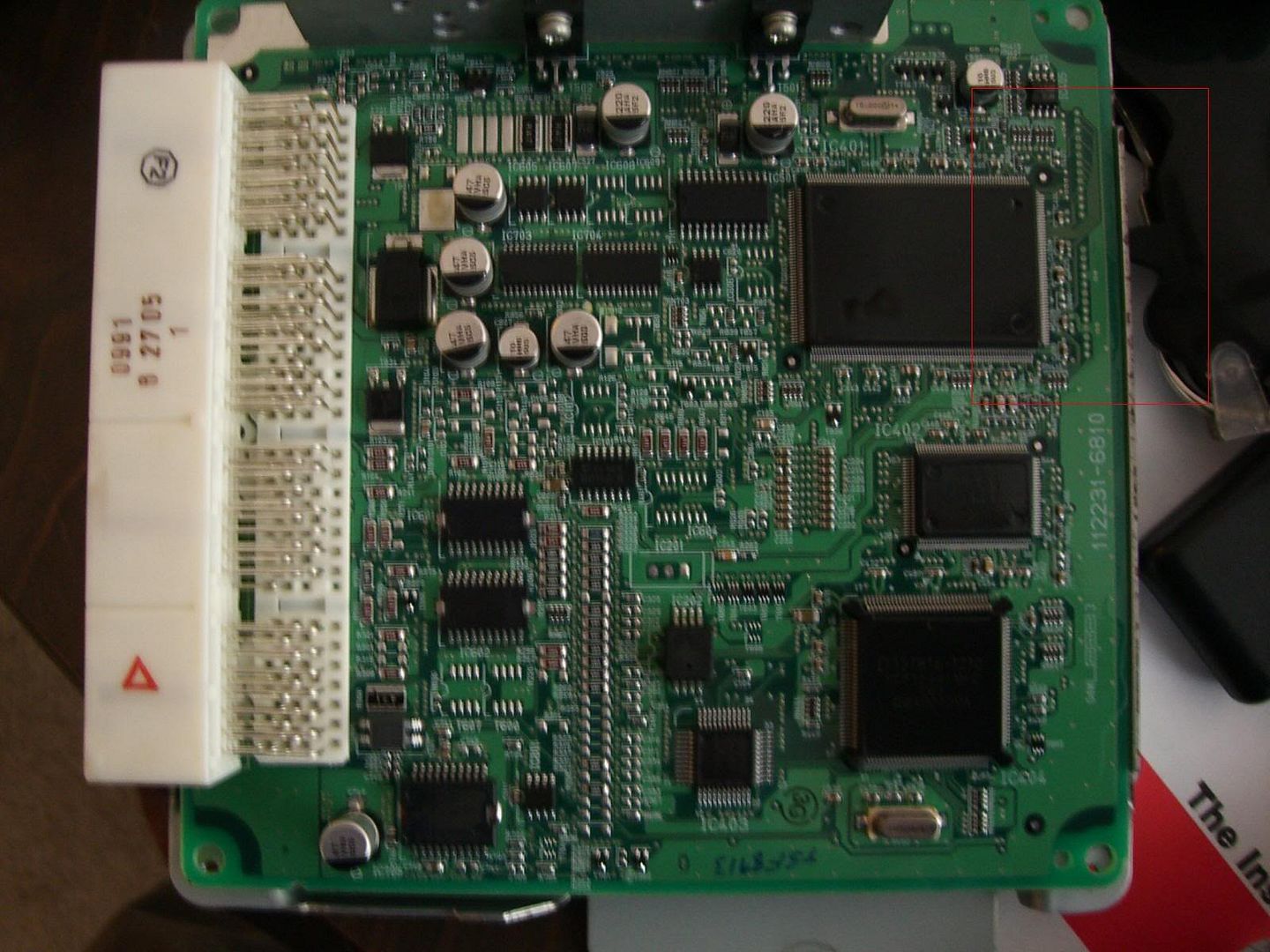
could I get a shot taken with the same exposure, focused in on that area? thats where the JTAG pins are, I'd like to see if denso made them easily accessible.
thanks!
|
|
| Top |
|
|
|
eamiller
|
Post subject: Posted: Thu Nov 16, 2006 12:19 am |
|
|
| Newbie |
Joined: Sat Oct 07, 2006 9:46 pm
Posts: 10
|
05GarnetLGT wrote: excellent!
now to identify in the photo which pins are jtag....
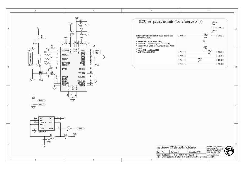
My guess, looking at the documentation and here http://www.codescape.com/processors.htm, is that jtag connection is possible via the H-UDI port which means the following pins are used:
Pin 236 - TCK (Test Clock input)
Pin 232 - TMS (Test Mode select)
Pin 234 - TDI (Test Data Input)
Pin 235 - TDO (Test Data Output)
Pin 233 - TRST (Test mode Reset active low)
|
|
| Top |
|
|
|
05GarnetLGT
|
Post subject: Posted: Thu Nov 16, 2006 12:21 am |
|
|
| Experienced |
Joined: Fri Feb 10, 2006 4:41 pm
Posts: 483
Location: toggle switch envy, PA
|
|
right, they are in the middle of that red rectange; what I mean is, did denso leave some unmasked vias for us(them originally) to solder to in order to debug?
|
|
| Top |
|
|
|
eamiller
|
Post subject: Posted: Thu Nov 16, 2006 12:34 am |
|
|
| Newbie |
Joined: Sat Oct 07, 2006 9:46 pm
Posts: 10
|
05GarnetLGT wrote:
could I get a shot taken with the same exposure, focused in on that area? thats where the JTAG pins are, I'd like to see if denso made them easily accessible.
thanks!
Colby is reflashing it right now, but when it comes back I will get some better pictures.. If you count down from the top right, the H-UDI port begins on the 21st pin down. Without tracing through the vias, it looks like the lower set of vias are most likely.
The AUD port pins are likely the upper set of vias, although there are probably more than that in those vias. Generally, they have to be able to test every net after the board is assembled as part of the final-test procedure. So you either need a via or a testpoint.
|
|
| Top |
|
|
|
eamiller
|
Post subject: Posted: Thu Nov 16, 2006 12:41 am |
|
|
| Newbie |
Joined: Sat Oct 07, 2006 9:46 pm
Posts: 10
|
05GarnetLGT wrote: right, they are in the middle of that red rectange; what I mean is, did denso leave some unmasked vias for us(them originally) to solder to in order to debug?
Usually, they do have to have them pinned out for the test fixture to check for shorts/opens. Of course, it may be how they program at end-of-line.
Generally micros are programmed 1 of 2 ways at the end:
1. A basic bootloader is loaded into the IC, and the final program is put in through the communication bus (usually CAN, but can be any)
2. The program is flashed in the final test fixture through the vias. Of course, that leaves it open as to what port on the processor they use.
|
|
| Top |
|
|
|
05GarnetLGT
|
Post subject: Posted: Thu Nov 16, 2006 12:44 am |
|
|
| Experienced |
Joined: Fri Feb 10, 2006 4:41 pm
Posts: 483
Location: toggle switch envy, PA
|
eamiller wrote: 05GarnetLGT wrote: right, they are in the middle of that red rectange; what I mean is, did denso leave some unmasked vias for us(them originally) to solder to in order to debug? Usually, they do have to have them pinned out for the test fixture to check for shorts/opens. Of course, it may be how they program at end-of-line. Generally micros are programmed 1 of 2 ways at the end: 1. A basic bootloader is loaded into the IC, and the final program is put in through the communication bus (usually CAN, but can be any) 2. The program is flashed in the final test fixture through the vias. Of course, that leaves it open as to what port on the processor they use. where I work we use method 2 for most boards, method 1 for others, but all of the boards have JTAG sections pretty clearly marked on the boards.
|
|
| Top |
|
|
|
05GarnetLGT
|
Post subject: Posted: Fri Jan 05, 2007 1:09 am |
|
|
| Experienced |
Joined: Fri Feb 10, 2006 4:41 pm
Posts: 483
Location: toggle switch envy, PA
|
|
| Top |
|
|
|
salex
|
Post subject: Posted: Fri Jun 15, 2007 1:44 am |
|
|
| Newbie |
Joined: Tue Aug 29, 2006 2:30 pm
Posts: 4
|
|
LGT, do you have a high res version of the plans from Colby?
I will try to reach him, but since he is a very busy man, I doubt it will be easy for him to help...
|
|
| Top |
|
|
|
05GarnetLGT
|
Post subject: Posted: Sun Jun 17, 2007 11:34 pm |
|
|
| Experienced |
Joined: Fri Feb 10, 2006 4:41 pm
Posts: 483
Location: toggle switch envy, PA
|
|
no, sorry, I just got that picture from a post someone else made..
|
|
| Top |
|
|
Who is online |
Users browsing this forum: No registered users and 4 guests |
|
You cannot post new topics in this forum
You cannot reply to topics in this forum
You cannot edit your posts in this forum
You cannot delete your posts in this forum
You cannot post attachments in this forum
|

|